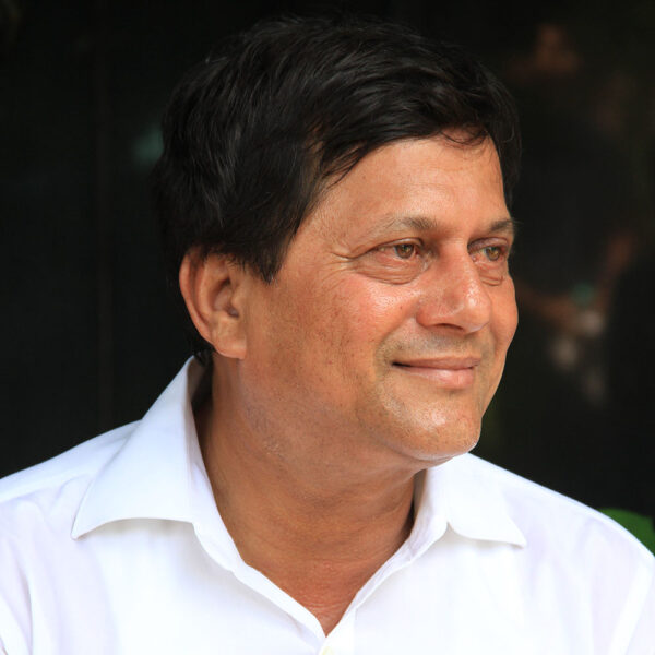
Subir Kumar Maity
Assistant Professor
Subir Kr. Maity has more than twelve years of academic experience. He has completed Ph.D. from the Institute of Radio Physics and Electronics, University of Calcutta, in the area of Nano-scale MOS transistors with III-V compound semiconductors as channel material. He has completed his M.Tech in specialization of VLSI Design and Microelectronics Technology from Jadavpur University, Kolkata, West Bengal. He is also the winner of the gold medal for securing 1st position in the M.Tech VLSI specialization. His search interests are compact modeling of sub-micron MOSFET, MOS transistors with high mobility channel material, quantum well MOSFET, Negative Capacitance FETs, Artificial Neural network based compact model development, etc.
Profile Links
Email :
[email protected]
Scopus Id :
57052324700
Google Scholar :
https://scholar.google.com/citations?user=7BuZx6wAAAAJ&hl=en
Social Links
VLSI Design & Microelectronics, Nano Scale MOSFET
Administrative Responsibility
FIC Exam co-ordinator
1. Cherik, I. C., Abbasi, A., Maity, S. K., & Mohammadi, S. (2023). Junctionless tunnel field-effect transistor with a modified auxiliary gate, a novel candidate for high-frequency applications. Micro and Nanostructures, 174, 207477.
2. Chowdhury, D., De, B. P., Maity, S. K., Singh, N. K., Kar, R., & Mandal, D. (2023). Performance Assessment of Graded Channel Gate-Stack based Double Gate MOSFET for Bio-sensing Applications. Silicon, 15(4), 1679-1689.
3. Ahmed, T., Shamim, S. U. D., Maity, S. K., & Basak, A. (2023). Performance evaluation of lead free CH3NH3SnI3/GeTe Tandem solar cell with HTL layer by SCAPS 1D. Optik, 282, 170836.
4. Das, H. S., Mishra, S., Dash, M. K., Kumar, P., Maity, S. K., Khatua, D., ... & Roymahapatra, G. (2023). Transparent Conducting Gallium-Doped Zinc Oxide Thin Films on Glass Substrate for Optoelectronic Device Applications. ES Materials & Manufacturing.
5. Maity, S.K, Basak, A, Das, HS. Study of scaling effect of ferroelectric gate stack in planar InGaAs MOSFET. Int J Numer Model. 2023; 36(2):e3059. doi:10.1002/jnm.3059
6. S.K. Maity, P. Dutta, S.Pandit, Compact drain current modeling of planar InGaAs quantum well MOSFET,Micro and Nanostructures, Volume 169, 2022, 207361, ISSN 2773-0123, https://doi.org/10.1016/j.micrna.2022.207361.
7. Rout, S.P., Dutta, P. & Maity, S.K. DC and RF analysis of a misaligned heterostructure GaSb//SiGe junctionless DG-MOSFET. Pramana - J Phys 96, 179 (2022).
8. Maity, S. K., & Pandit, S. (2022). Device-circuit analysis of ultra-thin body In1−xGaxAs on insulator MOS transistor with varying indium mole fraction and channel thickness. Engineering Research Express. http://iopscience.iop.org/article/10.1088/2631-8695/ac6ecc (in press, Accepted)
9. Rout, S. P., Dutta, P., & Maity, S. K. (2022). Improvement on the Performance of III-V Channel Based Ultra-Thin Junction-Less-Hybrid CMOS Circuits with Mixed Mode Analysis. ECS Journal of Solid State Science and Technology.
10. Maity, S. K., & Pandit, S. (2021). A SPICE compatible physics-based intrinsic charge and capacitance model of InAs-OI-Si MOS transistor. Superlattices and Microstructures, 156, 106975.
11. Toan, H. L. M., & Maity, S. K. (2021). Physics based compact modeling of symmetric double gate MOS transistors with high mobility III-V channel material. Superlattices and Microstructures, 155, 106925.
12. S. K. Maity, A. Haque and S. Pandit, "Charge-Based Compact Drain Current Modeling of InAs-OI-Si MOSFET Including Subband Energies and Band Nonparabolicity," in IEEE Transactions on Electron Devices, vol. 67, no. 6, pp. 2282-2289, June 2020. doi: 10.1109/TED.2020.2984578
13. Das, H.S., Das, R., Nandi, P.K. , Biring, S. and Maity, S.K., Influence of Ga-doped transparent conducting ZnO thin film for efficiency enhancement in organic light-emitting diode applications. Appl. Phys. A 127, 225 (2021). https://doi.org/10.1007/s00339-021-04339-6
14. Maity, S.K. Sub-Threshold Performance Assessment of Ultra-Thin Body InGaAs-on Insulator Negative Capacitance MOS Transistor. Silicon 12, 2681–2688 (2020). https://doi.org/10.1007/s12633-019-00364-6
15. Maity, S.K, Pandit, S. Analysis of scaling of thickness of the buffer layer on analog/RF and circuit performance of InAs‐OI‐Si MOSFET using NQS model. International Journal of Numerical modeling. 2020; 33:e2664. https://doi.org/10.1002/jnm.2664
16. Maity, S.K., Pandit, S. Performance Assessment of CMOS circuits using III-V on Insulator MOS Transistors. Silicon (2020). https://doi.org/10.1007/s12633-020-00582-3
17. Toan, H.L.M., Singh, S.S. & Maity, S.K. Analysis of Temperature Effect in Quadruple Gate Nano-scale FinFET. Silicon (2020). https://doi.org/10.1007/s12633-020-00615-x
18. S.K.Maity, S.Pandit, Study of G-S/D underlap for enhanced analog performance and RF/circuit analysis of UTB InAs-OI-Si MOSFET using NQS small signal model, Superlattices and Microstructures, Volume 101, 2017,Pages 362-372, ISSN 0749-6036, https://doi.org/10.1016/j.spmi.2016.11.053.
19. S.K.Maity & S.Pandit (2017) Effects of BOX engineering on analogue/RF and circuit performance of InGaAs-OI-Si MOSFET, International Journal of Electronics, 104:11, 1777-1794, DOI: 10.1080/00207217.2017.1312715
Conferences
1. E. Priyadarshini and S. Kumar Maity, "Performance Assessment of UTB-SOI MOS Transistor with Negative Capacitance Gate-stack," 2018 International Conference on Applied Electromagnetics, Signal Processing and Communication (AESPC), Bhubaneswar, India, 2018, pp. 1-4. doi: 10.1109/AESPC44649.2018.9033231
2. S. K. Maity and S. Pandit, "Compact drain current modeling of InAs-OI-Si MOS transistor including quantum confinement," 2018 International Symposium on Devices, Circuits and Systems (ISDCS), Howrah, 2018, pp. 1-5.doi: 10.1109/ISDCS.2018.8379654
3. A. Mishra, S. K. Maity and S. Dutta, "Effect of spacer dielectric of asymmetric underlap double gate MOSFET on SRAM performance," 2017 Devices for Integrated Circuit (DevIC), Kalyani, India, 2017, pp. 817-820. doi: 10.1109/DEVIC.2017.8074067
4. S. Dutta and S. K. Maity, "Temperature dependent analog/RF performance of double gate MOS transistor," 2016 International Conference on Signal Processing, Communication, Power and Embedded System (SCOPES), Paralakhemundi, 2016, pp. 834-837.
doi: 10.1109/SCOPES.2016.7955558
5. A. Mishra and S. K. Maity, "Influence of high-κ spacer on analog/RF performance of asymmetric underlap double gate MOSFET," 2016 International Conference on Signal Processing, Communication, Power and Embedded System (SCOPES), Paralakhemundi, 2016, pp. 653-656. doi: 10.1109/SCOPES.2016.7955522
6. V. Hemaja and S. K. Maity, "Impact of gate underlap on device performance of Germanium-on Insulator MOS transistor," 2016 International Conference on Electrical, Electronics, and Optimization Techniques (ICEEOT), Chennai, India, 2016, pp. 2051-2054. doi: 10.1109/ICEEOT.2016.7755048
7. S. K. Maity and S. Pandit, "Study of analog and RF performance of UTB-OI-Si substrate MOS transistor using buffered InGaAs and Silicon channel," 2015 6th International Conference on Computers and Devices for Communication (CODEC), Kolkata, India, 2015, pp. 1-4.
doi: 10.1109/CODEC.2015.7893193
8. B. S. Choudhury and S. K. Maity, "A 405MHz integer-N CMOS PLL for implantable biomedical application," 2015 IEEE 2nd International Conference on Recent Trends in Information Systems (ReTIS), Kolkata, India, 2015, pp. 509-513. doi: 10.1109/ReTIS.2015.7232932
9. A. Satapathy, S. K. Maity and S. K. Mandal, "A flipped voltage follower based analog multiplier in 90nm CMOS process," 2015 International Conference on Advances in Computer Engineering and Applications, Ghaziabad, India, 2015, pp. 628-631.
doi: 10.1109/ICACEA.2015.7164767
10. T. R. Devi, S. Maity and A. Datta, "A novel design of 4-bit distributed MEMS transmission line (DMTL) phase shifter using an RF shunt capacitive MEMS switch for phased array antenna," International Conference for Convergence for Technology-2014, Pune, India, 2014, pp. 1-6. doi: 10.1109/I2CT.2014.7092055
Books :
Maity, Subir Kumar, and Soumya Pandit. "UTB III–V-OI-Si MOS transistor: the future transistor for VLSI design." VLSI and Post-CMOS Electronics: Devices, circuits and interconnects 2, IET Digital library, (2019): 27.
- Researchgate: https://www.researchgate.net/profile/Subir-Maity
- Orcid: https://orcid.org/0000-0002-8825-996X

